Two-dimensional (2D) semiconducting materials have sparked significant interest in the field of electronics due to their potential applications in wearable devices and miniaturized electronics. These materials offer advantages over traditional bulky semiconductors, such as maintaining carrier mobility even with reduced thickness. While there has been progress in utilizing 2D semiconductors for thin electronics, the development of monolayer transistors, which are pivotal components for modulating and amplifying electrical current in devices, remains limited. Previous attempts at creating monolayer transistors relied on a handful of materials with stable lattice structures, like graphene or tungsten diselenide. Recently, researchers from Hunan University, the Chinese Academy of Sciences, and Wuhan University embarked on a quest to develop monolayer transistors using alternative 2D semiconducting materials that have been primarily used for multi-layer transistor designs.
Creating monolayer transistors with materials like black phosphorus (BP) and germanium arsenide (GeAs) pose challenges due to difficulties in forming stable electrical contacts with delicate 2D materials. In a recent publication in the journal Nature Electronics, Wangying Li, Quanyang Tao, and their colleagues outlined their strategy for fabricating monolayer BP and GeAs transistors with three-dimensional raised contacts by utilizing a van der Waals peeling technique. This work aimed to expand the scope of monolayer transistor designs beyond the commonly employed materials and explore the potential of less traditional 2D semiconductors. However, scaling down these materials uniformly without compromising their intrinsic properties proved to be a formidable task.
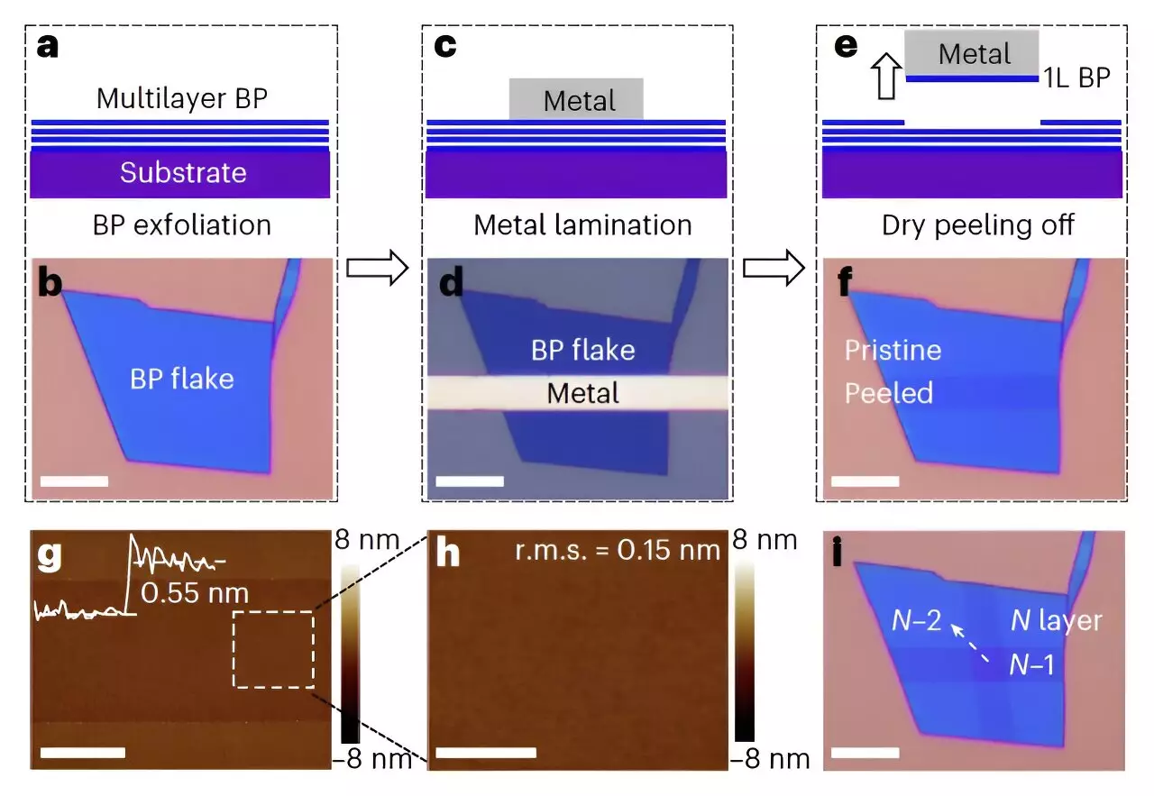
To overcome the challenges associated with new materials, Li, Tao, and their collaborators devised a van der Waals (vdW) peeling technique. This technique involves laminating flat metals onto multilayer 2D channels, enabling the removal of the semiconducting layer at the top by peeling off the metal. By utilizing layer-by-layer mechanical peeling, the researchers successfully reduced the channel region of multilayer black phosphorus transistors to monolayer thickness while preserving the delicate lattice in the multilayer contact region. In their study, the team applied this peeling technique to create homo-junctions and homo-superlattices using various 2D semiconductors such as BP, GeAs, InSe, and GaSe. Through this process, they demonstrated the ability to thin down the channel part of the transistors while maintaining the required thickness in the contact region.
By employing the proposed peeling technique, the researchers were able to measure the electrical properties of the same 2D transistor with different channel thicknesses. They discovered that the carrier mobility of black phosphorus decreased significantly when the body thickness was reduced, behaving more like a conventional bulk semiconductor rather than a pure van der Waals semiconductor. This finding sheds light on the behavior of 2D semiconductors under varying thicknesses and is crucial for understanding their potential in electronic applications.
The Future of Thinner and Scalable Transistors
The recent study by Li, Tao, and their colleagues demonstrates the potential of the layer-by-layer peeling method for developing promising monolayer transistors with 3D-raised contacts using materials like BP and GeAs. Furthermore, this technique could unlock new possibilities for creating thinner and scalable transistors using unconventional 2D semiconductors, which were previously considered poorly performing for these applications. The researchers envision that their work has implications not only for 2D semiconductors but also for other unstable monolayer materials such as organic monolayers and perovskite monolayers. These materials, often perceived as non-conductive or possessing poor intrinsic properties, may actually be limited by the poor contact between the metal and monolayers.
The quest for thinner and scalable transistors is driving researchers to explore the untapped potential of 2D semiconductors. By utilizing a novel van der Waals peeling technique, Li, Tao, and their collaborators have successfully fabricated monolayer transistors with 3D raised contacts using alternative materials like BP and GeAs. This breakthrough opens up new horizons for the development of thinner electronics and encourages the investigation of other monolayer materials beyond 2D semiconductors. In the future, advancements in peeling methods may pave the way for the integration of unconventional 2D semiconductors into a wide range of electronic applications, revolutionizing the field of miniaturized and wearable devices.


Leave a Reply