The realm of semiconductor technology has long captivated researchers and engineers alike. At its heart lies the behavior of electric charges as they interact across the interface of different semiconductor materials. Recent groundbreaking work led by researchers at UC Santa Barbara introduces a unique perspective on this interaction, capturing the first-ever “movie” showcasing the movement of electric charges. This development not only expands our understanding of charge dynamics but also offers practical implications for the design and efficiency of semiconductor devices.
Photocarriers form the basis of many modern electronic devices, with applications ranging from solar cells to lasers. The process begins when light strikes a semiconductor, exciting electrons, which then create a flow of current through the material. However, this flow is often transient, with most energy dissipating as waste heat within a mere trillionth of a second. Researchers are eager to harness the potential energy of these “hot” carriers before they cool down, yet understanding their behavior at atomic levels remains a substantial challenge.
As the researchers at UC Santa Barbara discovered, traditional methods of measuring carrier dynamics have largely relied on indirect observations, leaving a gap in the ability to observe these critical processes directly. Associate Professor Bolin Liao, who led the research, emphasized the novelty of visualizing these fast-moving charges in actionable scenarios.
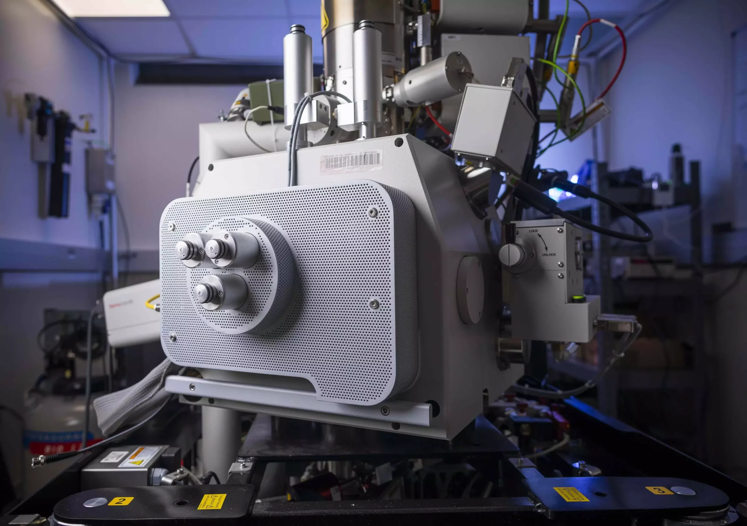
The team employed a sophisticated technique known as scanning ultrafast electron microscopy (SUEM) to capture the behavior of hot carriers. By synchronizing ultrafast laser pulses with an electron beam, they were able to take snapshots of the carriers in the critical picosecond to nanosecond range. This pioneering method is akin to adding time resolution to conventional electron microscopy, significantly enhancing the potential to analyze real-time phenomena in semiconductor materials.
The focus of the imaging was a heterojunction composed of silicon and germanium—two widely used semiconductor materials whose interface plays a critical role in the effectiveness of various devices, from photovoltaic cells to advanced telecommunication systems.
Understanding how charge carriers behave at heterojunctions is crucial for designing more efficient semiconductor devices. As Liao noted, the behavior of carriers fluctuates under different circumstances. For example, when charges are generated in uniform regions of silicon or germanium, they exhibit rapid movement. However, at the junction, a significant portion of these hot charges becomes trapped, leading to decreased mobility.
This trapping phenomenon introduces a range of challenges for engineers aiming to optimize device performance. Addressing it could unlock new pathways to more efficient energy conversion in photovoltaic systems, spotlighting the importance of this research not simply as theoretical knowledge, but as a foundational influence on practical outcomes in technology.
The work performed at UC Santa Barbara encapsulates a remarkable journey that dates back to the pioneering concepts of heterostructures proposed by Herb Kroemer in 1957. His assertion that “the interface is the device” laid the groundwork for what has become the backbone of modern electronics. The recent ability to visualize charge movements at these interfaces completes a critical circle in semiconductor research, bridging historical concepts and contemporary advancements.
This research holds the potential for transformative impacts in the semiconductor field. As Liao and his team demonstrate the SUEM technique’s capabilities, it opens avenues for further experimental inquiries into the behavior of charge carriers across a variety of junctions and configurations.
As the landscape of technology continues to evolve, the insights garnered from the direct observation of hot carriers across heterojunctions pave the way for subsequent advancements in semiconductor research. This breakthrough directs attention toward not only understanding the fundamental behaviors of materials on an atomic scale but also the applications that arise from such knowledge.
The researchers aim to utilize this newfound ability to explore viable designs for next-generation semiconductor devices, pushing the boundaries of what we currently understand about materials science. By enhancing our capability to visualize and analyze charge behaviors at nanometer scales, the implications for improved energy efficiency, faster electronics, and innovative technologies appear promising.
The pioneering efforts of UC Santa Barbara researchers signify a landmark advancement in semiconductors, providing rich insights into the dynamics of charge carriers that could shape the future of electronics. The convergence of innovative imaging techniques and deep theoretical understanding heralds a new era of discovery in the field, reaffirming the essential role semiconductor materials play in driving technological progress.
Leave a Reply