The field of photonic integrated circuits is rapidly advancing, with a focus on miniaturizing photonic elements and integrating them into chips that can carry out calculations using photons instead of electrons. Silicon-based photonics is a promising area that has applications in data centers, artificial intelligence, quantum computing, and more. This technology offers significant improvements in performance and cost-benefit ratios, leveraging the well-developed lithography production process. However, one of the major challenges in this field is accurately mapping the optic characteristics of photonic chips.
Photonic circuits operate at a tiny scale, making it difficult to model the impact of fabrication flaws and inaccuracies on the chip’s performance. The current instruments used for mapping the internal light motion of these chips do not provide accurate results due to the devices’ small dimensions. This limitation hampers the design and optimization processes for photonic chips in various fields.
A group of researchers from Technion’s Andrew and Erna Viterbi Faculty of Electrical and Computer Engineering has made significant progress in addressing this challenge. Led by Professor Guy Bartal and doctoral student Matan Iluz, the team developed a groundbreaking technique for advanced light imaging in photonic circuits on chips. The results of their research were published in the journal Optica.
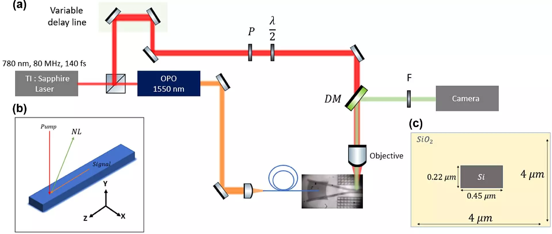
The researchers utilized the optical characteristics of silicon to map the propagation of light waves without the need for invasive actions that could potentially alter the chip. By studying the electric field of the light waves and identifying the elements that impact its movement, such as waveguides and beam splitters, the team was able to generate real-time images and video recordings of the light inside the photonic chip.
One of the key advantages of this new technique is that it does not require damaging the chip or losing any data. By non-invasively mapping the light’s propagation, the researchers have overcome a significant barrier in accurately characterizing photonic chips. This breakthrough is expected to have wide-ranging implications for the design, production, and optimization processes of photonic chips in fields such as telecommunications, high-performance computing, machine learning, medical imaging, sensing, and quantum computing.
The field of photonic integrated circuits has taken a major step forward with the development of a new technique for advanced light imaging. Researchers at Technion have successfully harnessed the optical characteristics of silicon to non-invasively map the light’s propagation inside photonic chips. This breakthrough will greatly enhance the design, production, and optimization of photonic chips, leading to improved performance and cost-efficiency in various industries. The future of photonic circuits looks brighter than ever, with possibilities for further advancements in telecommunications, computing, healthcare, and quantum technologies.


Leave a Reply