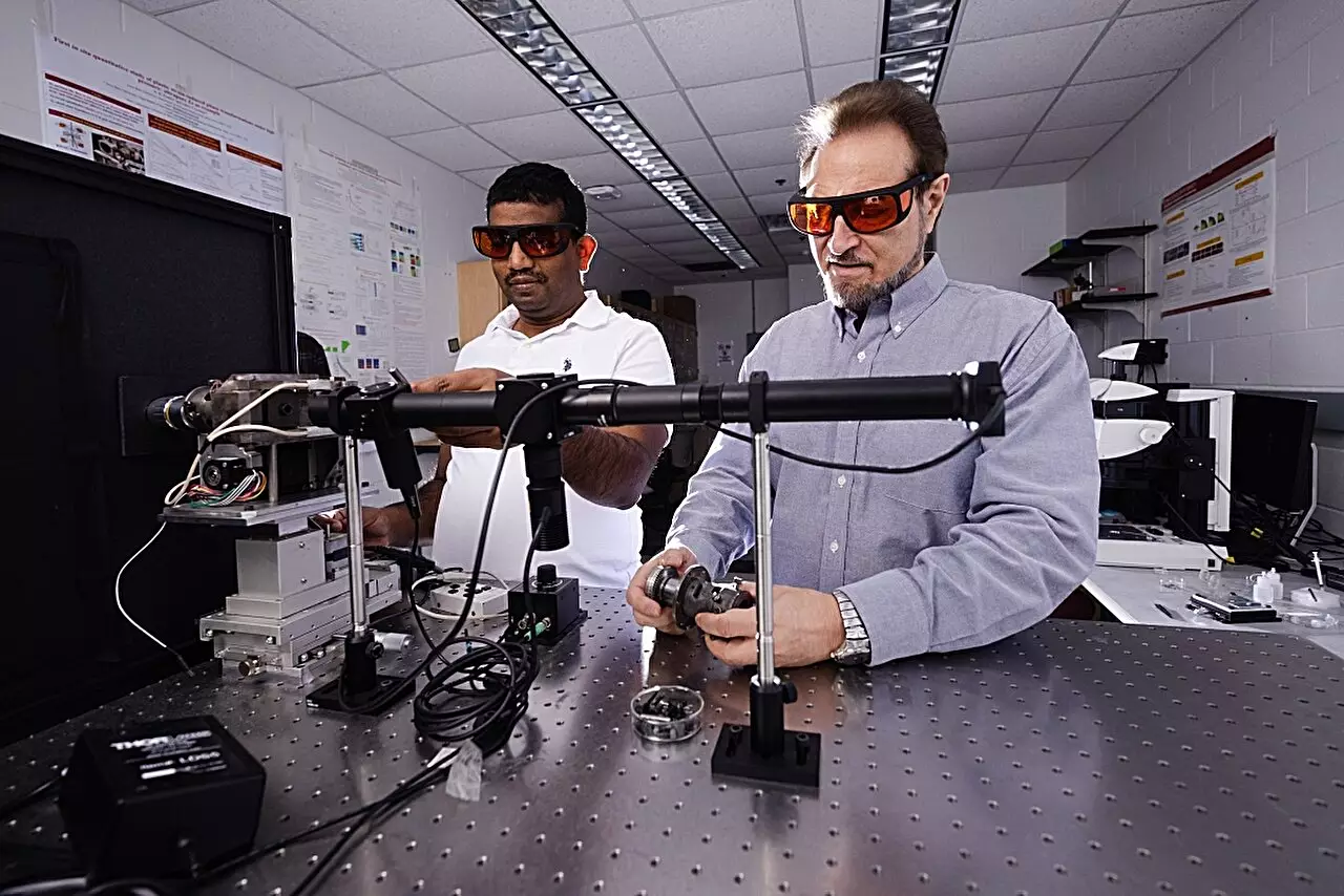
In the realm of materials science, the marriage of theoretical understanding and experimental verification is crucial for pioneering advancements. Valery Levitas, a distinguished professor at Iowa State University, has taken significant strides in this field since his arrival in the United States from Europe in 1999. His journey began with a rotational diamond anvil cell, a sophisticated instrument designed to apply immense pressure on materials between diamond tips. This tool has since evolved, allowing researchers to conduct in situ examinations of how materials behave under extreme conditions. This article delves into Levitas’ groundbreaking research on silicon and its unexpected behavior under conditions of pressure and shear deformation.
Silicon has long held its status as a cornerstone of modern electronics, often cited as the backbone of semiconductors. Given its ubiquitous presence, understanding its behavior under various physical conditions is paramount. Traditional research has focused predominantly on silicon’s transformations under high-pressure environments. However, Levitas and his colleagues approached the material from a novel angle by investigating its response not just to pressure, but also to plastic shearing—a method that has been largely overlooked in prior studies.
This innovative approach is especially relevant as industries increasingly seek efficient methods for material manipulation. By observing the effects of shearing in conjunction with pressure, researchers aim to uncover potential new properties that could advance silicon’s applications beyond current capabilities.
Recent findings from this research team, published in the prestigious journal Nature Communications, challenge established norms within materials research. They focused on three distinct particle sizes of silicon, ranging from 1 millionth of a meter to 100 billionths of a meter. Levitas’ team subjected these silicon samples to unique strains facilitated by the rotational diamond anvil cell and discovered that lower pressures could induce significant phase transformations. Their observations revealed that applying just 0.3 gigapascals in conjunction with plastic deformations caused a transformation from silicon’s “Si-I” phase to “Si-II”—a transition that typically occurs at much higher pressures of approximately 16.2 gigapascals.
Such a substantial reduction in the pressure required for this transformation signals a notable breakthrough. Levitas articulated the significance of this finding: “One of our goals is to reduce transformation pressures.” This reduction opens up new avenues for industrial applications, highlighting the potential for more practical implementations of high-pressure phases typically deemed impractical in conventional industrial settings.
Central to Levitas’ research is the concept of microstructural alteration rather than mere size or shape modification of material samples. It is well understood that introducing plastic deformations can lead to changes in the microstructure of silicon. These microscopic variations are what initiate the phase transformations and subsequently result in yield different physical properties. The paper discusses seven phases of silicon and the potential properties each can exhibit, which can be leveraged in various technological industries, including electronics and optics.
This approach could allow for the development of nanostructured materials—known as nanocomposites—that exhibit optimal electronic, optical, and mechanical properties. Such materials can revolutionize industries by enabling the production of devices that are not only more efficient but also robust and versatile.
Levitas’ innovative research is set against the backdrop of nearly two decades of exploration and theorization about material behavior under extreme conditions. His anticipatory hypothesis regarding silicon’s response to shear has now been validated through rigorous experimentation, reinforcing the significance of creative thinking in scientific inquiry.
As ongoing research continues to unravel complex material behaviors, the implications for engineering and industrial processes are vast. Levitas’ research heralds a new paradigm where conventional methods of high-pressure materials science are rendered more viable through the application of lower pressures and shear deformation. This advancement does not merely dazzle the academic community but has the potential to impact real-world applications significantly.
Through strategic experimentation and a willingness to explore uncharted territories within materials science, Levitas and his team are pioneering new frontiers in silicon research. The innovations stemming from their findings could lay the groundwork for the next generation of electronic materials and devices.


Leave a Reply