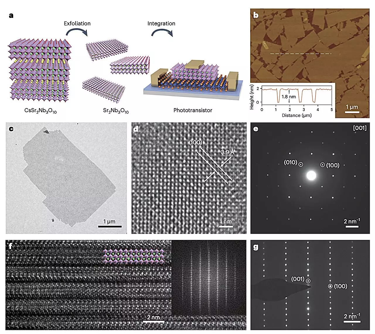
In the quest to develop smaller, more efficient optoelectronic devices, researchers have identified the need for higher gate capacitance to reduce energy consumption. This necessitates the use of insulating materials with a high dielectric constant (κ), such as hafnium oxide (HfO2), to maximize charge storage capacity. However, integrating these high-κ materials with two-dimensional (2D) semiconductors has proven to be a significant challenge.
A recent study by researchers at Fudan University has introduced a novel solution to this integration hurdle. By synthesizing a 2D perovskite oxide, Sr2Nb3O10, with a high κ of 24.6, they have demonstrated compatibility with a variety of 2D channel materials. This breakthrough paves the way for enhanced gate control and improved performance in miniaturized optoelectronic devices.
The unique properties of Sr2Nb3O10, including its high dielectric constant and moderate bandgap, make it an ideal candidate for use in phototransistors based on 2D semiconducting materials like graphene, molybdenum disulfide, and tungsten disulfide. The researchers were able to achieve impressive results, such as an on/off ratio of 106 and a photocurrent-to-dark-current ratio of ~106, by integrating Sr2Nb3O10 with these channel materials.
One of the most exciting findings of the study was the ability to distinguish between UV and visible light illumination using phototransistors with Sr2Nb3O10. This dual-band photodetection, made possible by the interface between the semiconductor and dielectric, opens up new possibilities for more advanced optoelectronic applications.
The success of integrating Sr2Nb3O10 with various 2D channel materials underscores the potential for further research in the field of 2D perovskite oxides. As researchers like Li and Liu continue to explore new synthesis methods and integration techniques, we can expect to see even more advancements in the development of smaller, more efficient, and energy-saving electronics and optoelectronics.


Leave a Reply